Software (LED Optimization Simulation)
-Virtual Reactor: Optimization: Reactor geometry and growth process parameters
MOCVD : III-V and III-N thin film growth optimization 2D Simulation
HVPE: GaN bulk and GaN thin film growth optimization 2D Simulation
-CVDSim NE: add on 3D Simulation coupled with FLUENT and CFD Ace+:
-STREEM: Strain&Dislocation Engineering Simulation of AlGaN and InGaN material
-SimuLED(SiLENSe(2D-epi:LED/LD),SpeCLED(3D chip), RATRO(3D ray tracing)): LED Simulation
-SimuLamp: LED Package level 3D Simulation
-FETIS: Field Effect Transistor Simulation
-PVCell: Semiconductor Photo Voltaic Cell Simulation
-BESST: Bandgap Engineering Superlattice Simulation Tool
Hardware (Nano Materials and Device)
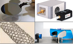
-Nano particles: SWCNT, MWCNT, Graphene, Nano powder
-Semiconductor wafers: Substrate and epi wafer with III-V and III-N
-NDT(Non Destructive Testing) Device:
Sub-THz and THz 2D&3D image Scanner system:
Radar system